Electronics and Semiconductors
Advanced Manufacturing for Electronics and Semiconductors
Advanced manufacturing for electronics and semiconductors focuses on cutting-edge technologies like precision robotics, automation, and AI-driven processes to produce high-performance, miniaturized components. Techniques include photolithography, wafer fabrication, and 3D integration. Emphasis on cleanrooms, materials innovation, and sustainability ensures efficiency and quality for devices like chips and sensors.

Electronics and Semiconductors Capabilities
Design and Development
- Advanced semiconductor design including SoCs, ASICs, and FPGAs.
- High-frequency circuit design for 5G, IoT, and RF applications.
- PCB and multi-layer design with thermal and EMI optimization.
Fabrication and Processing
- Wafer fabrication at leading-edge nodes (e.g., 3nm, 5nm, and 7nm).
- Specialized materials such as silicon carbide (SiC) and gallium nitride (GaN) for high-power and high-efficiency applications.
- Advanced photolithography techniques, including EUV for fine feature patterning.
Packaging Technologies
- System-in-Package (SiP) and chiplet integration.
- Fan-out wafer-level packaging (FOWLP) for size reduction.
- Advanced thermal management solutions for high-power chips.
Testing and Reliability
- Automated Test Equipment (ATE) for functional and parametric testing.
- Burn-in testing, thermal cycling, and accelerated aging tests.
- Defect detection using AI-based inspection systems.
Automation and AI Integration
- Robotic process automation (RPA) in assembly and production lines.
- Machine learning for predictive maintenance and yield optimization.
Materials Science Innovation
- High-purity materials for epitaxial growth.
- Research on flexible electronics and organic semiconductors.
Sustainability and Energy Efficiency
- Development of low-power chips for greener technologies.
- Recycling programs for rare earth metals and electronic waste reduction.
Top Electronics and Semiconductors Applications
Top Applications of Electronics and Semiconductors span diverse industries, enabling innovation and driving global progress:
- Consumer Electronics
- Automotive
- Telecommunications
- Industrial Automation
Consumer Electronics
- Smartphones, tablets, and laptops.
- Wearables like smartwatches and fitness trackers.
- Smart home devices (e.g., IoT appliances, smart speakers).
Automotive
- Advanced Driver Assistance Systems (ADAS).
- Electric vehicles (EVs) and hybrid powertrain systems.
- Sensors for autonomous driving and in-vehicle infotainment systems.
Telecommunications
- 5G infrastructure, including base stations and antennas.
- High-speed networking devices (routers, modems).
- Optical communication systems and satellite networks.
Industrial Automation
- Robotics, programmable logic controllers (PLCs).
- Sensors and actuators for smart factories (Industry 4.0).
- Power electronics for energy-efficient manufacturing equipment.
Electronics and Semiconductor Manufacturing Services
CNC Machining
- CNC Machining
- CNC Milling
- CNC Turning
Injection Molding
- Injection Molding
- Insert Molding
- Overmolding
Sheet Metal
- Sheet Metal Fabrication
- Waterjet Cutting
- Laser Cutting
- Plasma Cutting
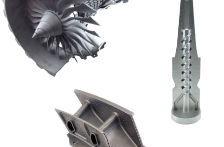
3D Printing
- Binder Jetting
- Carbon DLS
- Direct Metal Laser Sintering (DMLS)
- Fused Deposition Modeling (FDM)
- HP Multi Jet Fusion
- Polyjet
- Selective Laser Sintering (SLS)
- Stereolithography (SLA)
Why Choose Avinyaworks for Electronics and Semiconductor
Endless Options
Choose from millions of possible combinations of materials, finishes, tolerances, markings, and certifications for your order.
Easy to Use
Get your parts delivered right to your door without the hassle of sourcing, project management, logistics, or shipping.
Quality Assurance
Avinyaworks ensures aerospace and defense quality with advanced testing and tailored solutions for reliability and safety.